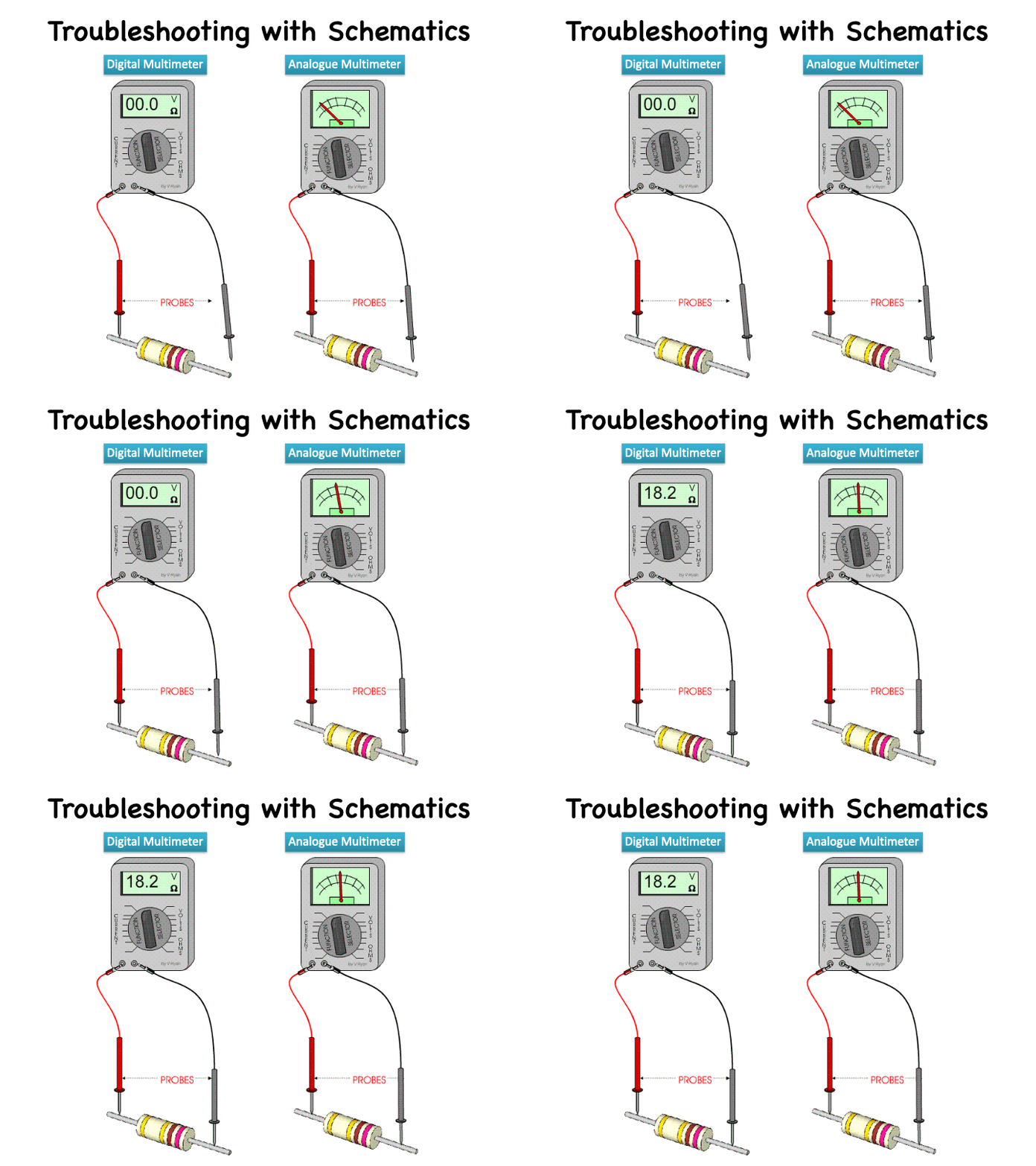
Here is a diagram for a somewhat more complicated, real-world electronic circuit presented in a form intended to assist a troubleshooting technician. The circuit has a single, NPN, bipolar transistor along with some resistors and capacitors. Note, that test points, (abbreviated TP), exist at three different locations. TP1 at the emitter of the transistor, TP2 at the base of the transistor, and TP3 at the collector of the transistor. If you need to troubleshoot this circuit, (which happens to be a low-power amplifier of the sort you might find in a vintage radio receiver or hi-fi set), you’ll connect your Volt-Ohm-Meter between chassis ground and each one of these three points in turn. You’ll carefully note the meter readings and compare them with known normal values.
This circuit receives a weak input AC signal, (such as the output of an ultrasonic pickup) and boosts it so that it can drive a device that consumes significant power, (such as a switching circuit). The general signal flow goes from left to right. The original AC signal enters at the input terminals, passes through capacitor C2, and reaches the base, (the left-hand electrode) of transistor Q1. The base acts as an adjustable “current valve”, that causes large current fluctuations through Q1 as the electrons flow from ground through R1 to the emitter, (the bottom electrode), then onward to the collector, (the top electrode), and out through R4 to the positive power supply terminal. Capacitors C2 and C3 allow the AC signals to pass while blocking DC from the power supply so that the DC won’t upset the operation of external circuits. Capacitor C1 keeps the transistor’s emitter at a constant DC voltage while allowing the input signal to enter unimpeded. The resistors R2 and R3 have values carefully chosen to place precisely the right DC voltage, called bias, on the base of Q1, ensuring that the transistor will work as well as it possibly can in this application.
In many electronic circuits, actual voltages can deviate from design values by up to 20 percent. If this information is important, you’ll usually find the error range at the bottom of the schematic drawing, or in the accompanying literature. If the readings obtained are within this known error range, (called the component tolerance), then you can tentatively assume that this part of the circuit is working properly. However, if the readings obtained are zero or well outside of the tolerance range, then you have pretty good reason to suspect a problem with the associated circuit portion, or possibly with other circuits that feed it.
Many schematic drawings that accompany electronic equipment, especially “projects” that you build from a kit containing individual components, include information that aids not only in troubleshooting but also in the initial testing and alignment procedures that you must follow as soon as you’ve completed the physical assembly process. As a further aid, the literature might include pictorial diagrams that show you where each part belongs on the circuit board or chassis. That way, you can follow the circuit not only according to its electrical details, but along the physical pathways as they actually look.
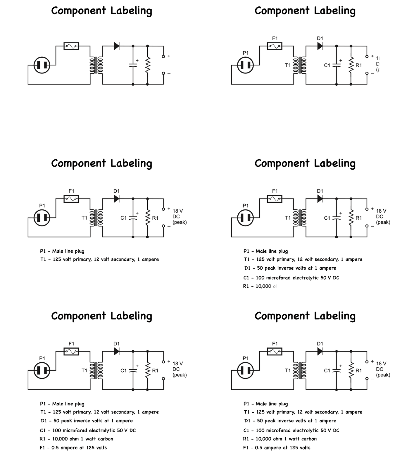
According to standard schematic drawing practice, every component should bear a unique alphabetic numeric label to designate it, as you see here. However, a few alternative labeling forms are also acceptable.


